Single Stage RC Coupled CE Amplifier
The figure shows a single stage CE amplifier. C1 and C3 are coupling capacitors, they are used for blocking the dc component and passing only ac part they also ensure that the dc basing conditions of the BJT remains unchanged even after input is applied. C2 is the bypass capacitor which increases the voltage gain and bypasses the R4 resistor for ac signals. The BJT is biased in the active region using the necessary biasing components. The Q point is made stable in the active region of the transistor. When input is applied as shown below the base current starts to vary up and down, hence collector current also varies as IC = β × IB. Therefore voltage across R3 varies as the collector current is passing through it. Voltage across R3 is the amplified one and is 180° apart from the input signal. Thus voltage across R3 is coupled to the load and amplification has taken place. If the Q point is maintained to be at the centre of the load very less or no waveform distortion will take place. The voltage as well as current gain of the CE amplifier is high (gain is the factor by which the voltage of current increases from input to output). It is commonly used in radios and as low frequency voltage amplifier.
To further increase the gain multistage amplifiers are used. They are connected via capacitor, electrical transformer, R-L or directly coupled depending on the application. The overall gain is the product of gains of individual stages. Figure below shows a two stage CE amplifier. various parameters of CE amplifier are
| Definition | Expression (with emitter degeneration) | Expression (without emitter degeneration, i.e., RE = 0) | |
|---|---|---|---|
| Current gain |  |  |  |
| Voltage gain |  | 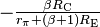 |  |
| Input impedance |  | 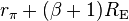 |  |
| Output impedance |  |  |  |
If you had financial problems, then it is time for you to smile. You only need to contact Mr. Benjamin with the amount you wish to borrow at the low rate of 2% ROI and the payment period that suits you and you will have your loan within three working days. I just benefited for the sixth time a loan of 700 thousand dollars for a period of 180 months with the possibility of paying before the expiration date. Mr Benjamin has been helping me with the loan.Make contact with him and you will see that he is a very honest man with a good heart.His email is 247officedept@gmail.com and his WhatApp phone number is + 1-989-394-3740 .
ReplyDelete